



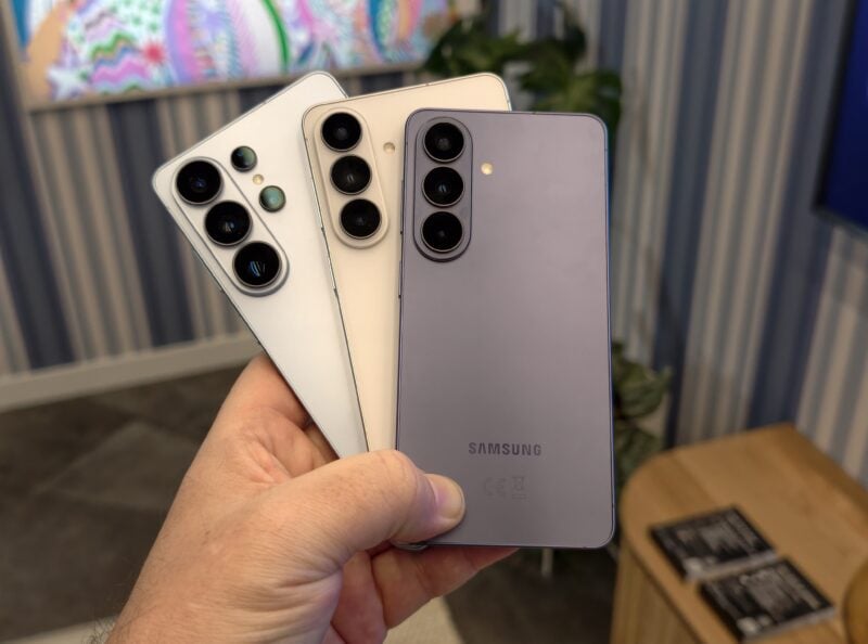
Two of the biggest names in hardware have made headlines this week. Samsung is reportedly producing its 400-layer 10th-generation NAND flash memory, while Huawei has unveiled its 122TB enterprise SSD built entirely around a proprietary Die-on-Board packaging method using domestic YMTC memory. Here's what that means for you.
Samsung has tripled phone storage capacity
A new leak from Ice Universe, who's among the most reliable Samsung tipsters in the industry, suggests that Samsung Electronics has successfully developed the world's first 900-layer V-NAND prototype. If it's accurate, it could be the most significant storage breakthrough in years.

V-NAND, or Vertical NAND, is the 3D flash memory inside every modern smartphone. Manufacturers stack them vertically to have more layers. Hence, the more storage you can fit into the same physical space without making the chip larger or more expensive.
The chips in flagship phones currently are built on roughly 300 to 321 layers. Samsung's prototype is nearly triple what they achieved by fusing two 450-layer wafers together. The development should bring 2TB to reality or maybe just faster memory and efficient storage as a standard on many phones outside the premium tier.
Higher density NAND could also allow for true on-device AI processing where most large models today lean on the cloud. However, based on the current pace of development, industry observers don't expect 900-layer technology to land inside a consumer phone before 2030 or 2032.
Huawei's exile produced its best weapons yet
Huawei's longtime exile from global semiconductor technology would've spelt the slow, managed decline of the company. Frankly, it has been so drawn out that you probably don't even remember how it started.
Back in 2019, the US Department of Commerce added the company to its Entity List on the grounds of national security tied to Chinese military and intelligence services. It cut them off from American technology and any foreign products built using American intellectual property. So they couldn't access TSMC chips, Qualcomm processors, advanced NAND from suppliers like Samsung, and use Google services on their phones.

It's been seven years later, and as this week made clear, there is always a way. Being blocked from the world's best tools has taught them how to build new ones. In the span of two days, they revealed a 122TB enterprise SSD built without advanced Western components.
Huawei’s figured out how to extract significantly more storage density from chips that are inferior to what the rest of the industry uses, all without adding more layers or relying on advanced manufacturing. It could mean phones getting more storage at lower cost and with less power consumption.
Specifically, it will cut data transfer power consumption by 80% in facilities that run thousands of drives simultaneously and pay enormous electricity bills to keep them running cool. They used a proprietary Die-on-Board packaging method that mounts bare memory dies directly onto the circuit board to squeeze 33% more density out of domestic YMTC chips.
The company's chip chief He Tingbo also announced LogicFolding, a new semiconductor architecture that abandons the geometric scaling principle the entire industry has operated on for decades. They've replaced it with what Huawei calls time scaling.
Since the 1960s, shrinking the transistors was the best way to fit more of them onto the same piece of silicon to boost performance. Time scaling compresses signal propagation delay to improve transistor density without shrinking anything physically.
If you attack the lag traveling between transistors on a chip and compress it, you'll get more computational work done in the same amount of time and with the same physical transistor size. The first chip built on this architecture lands in a flagship device this fall. A version targeting 1.4nm-equivalent density is on the roadmap for 2031.